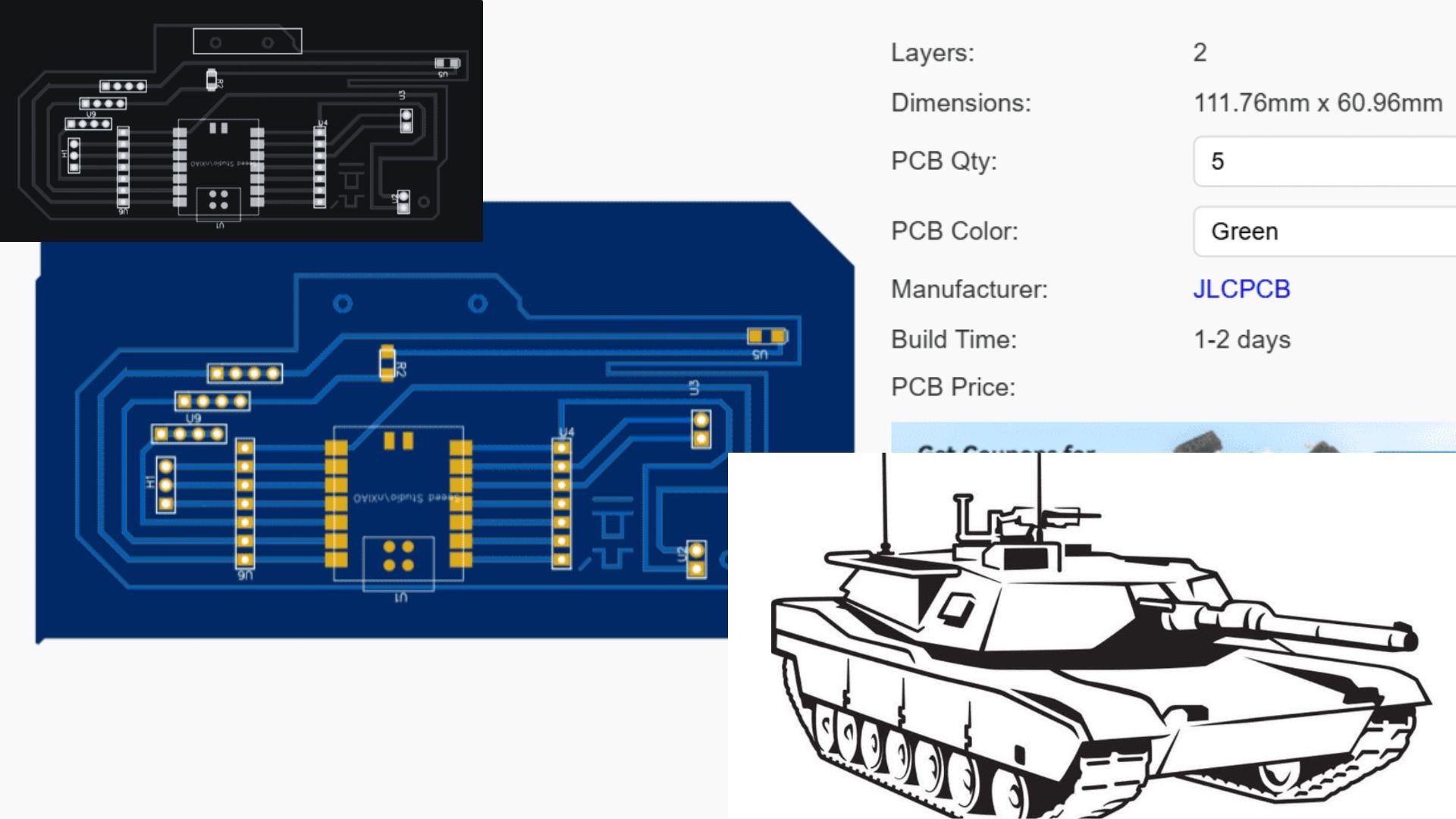
Tank-Shaped PCB
This project documents first experience designing and fabricating a circuit board, developed as a custom tank-shaped form.
Year:
2024
Category:
Digital Fabrication
Client:
Academic Project
Circuit Design
The process began with creating a schematic that defines how the circuit functions.
Components used:
Microcontroller (XIAO RP2040)
LEDs (output indicators)
Resistors (current limiting)
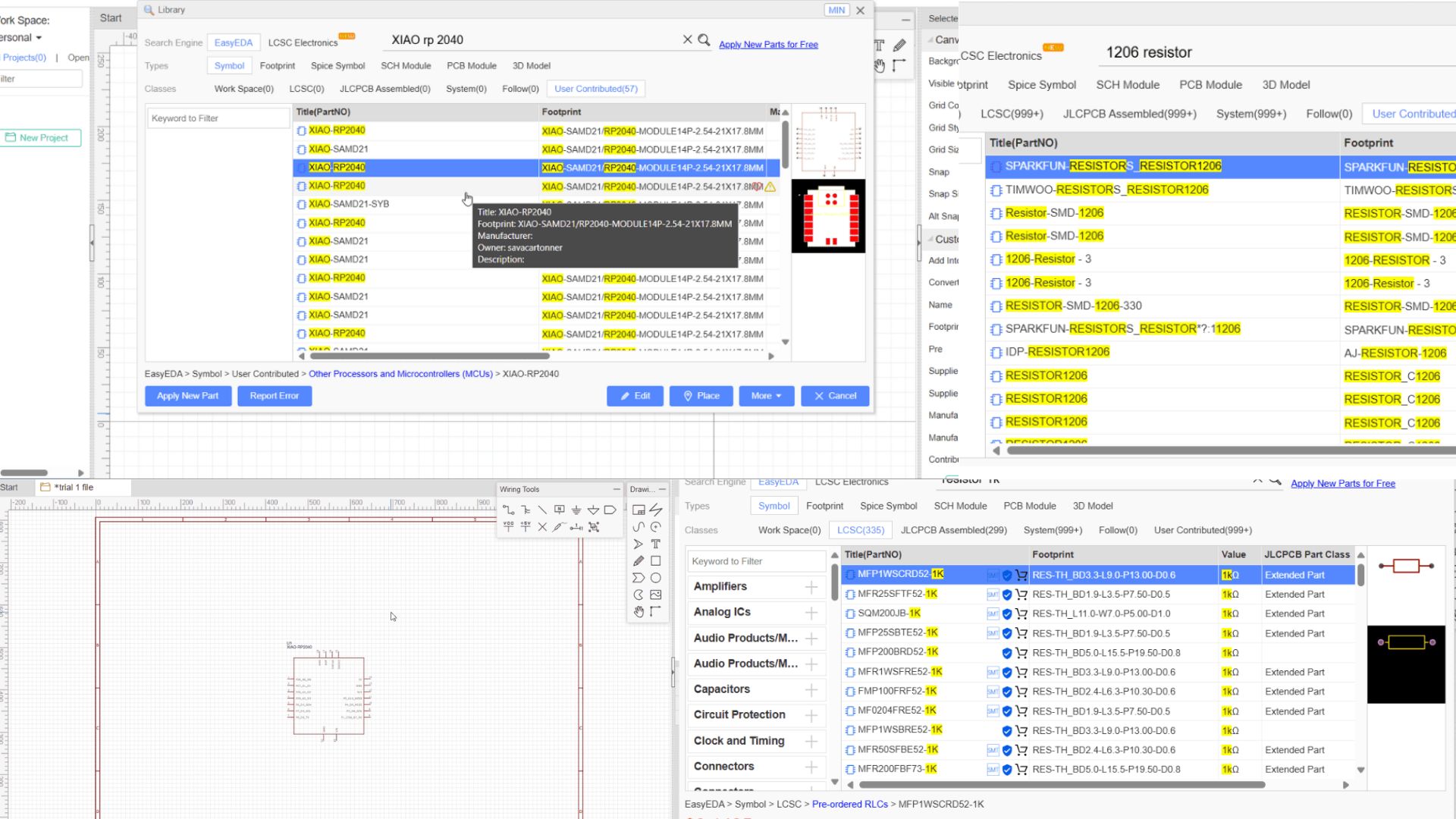
Software Used
Easy EDA, Copper CAD
Steps involved:
Defined power connections (VCC and GND)
Connected LEDs to GPIO pins through resistors
Ensured correct polarity of LEDs
Organized schematic for readability
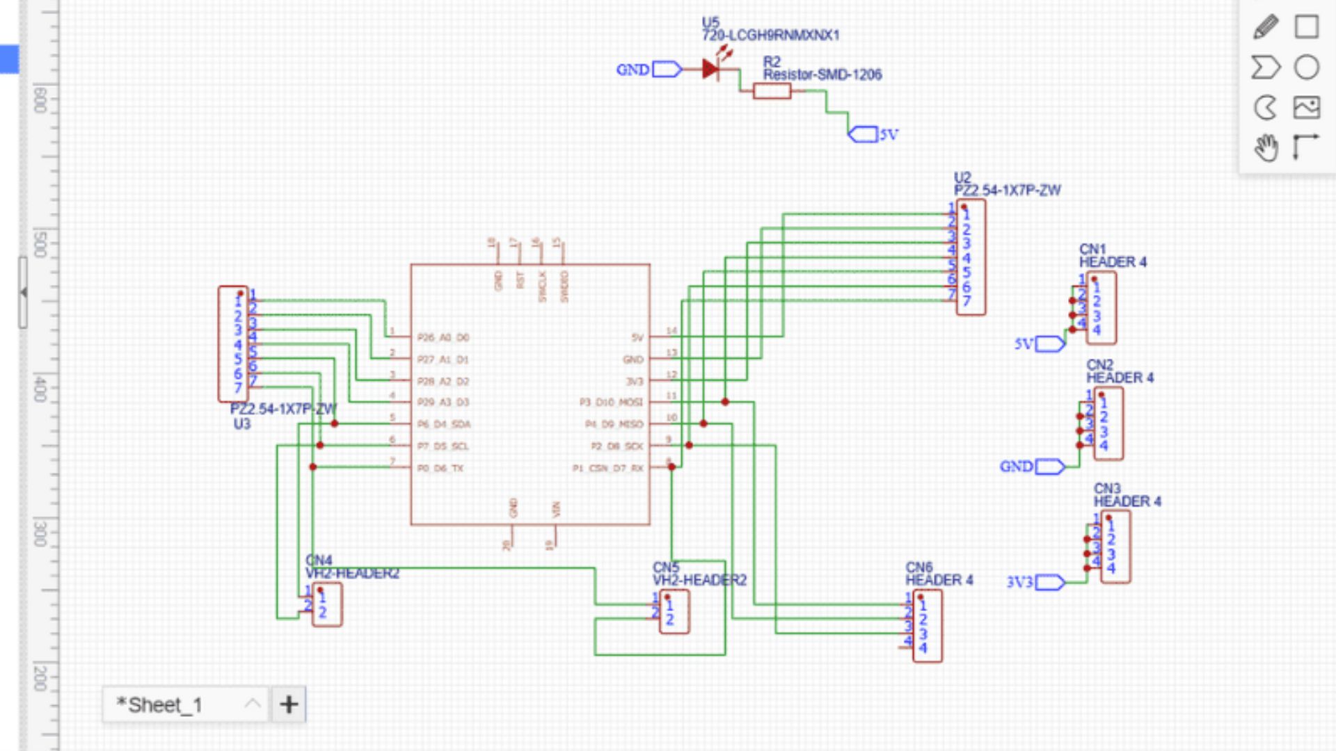
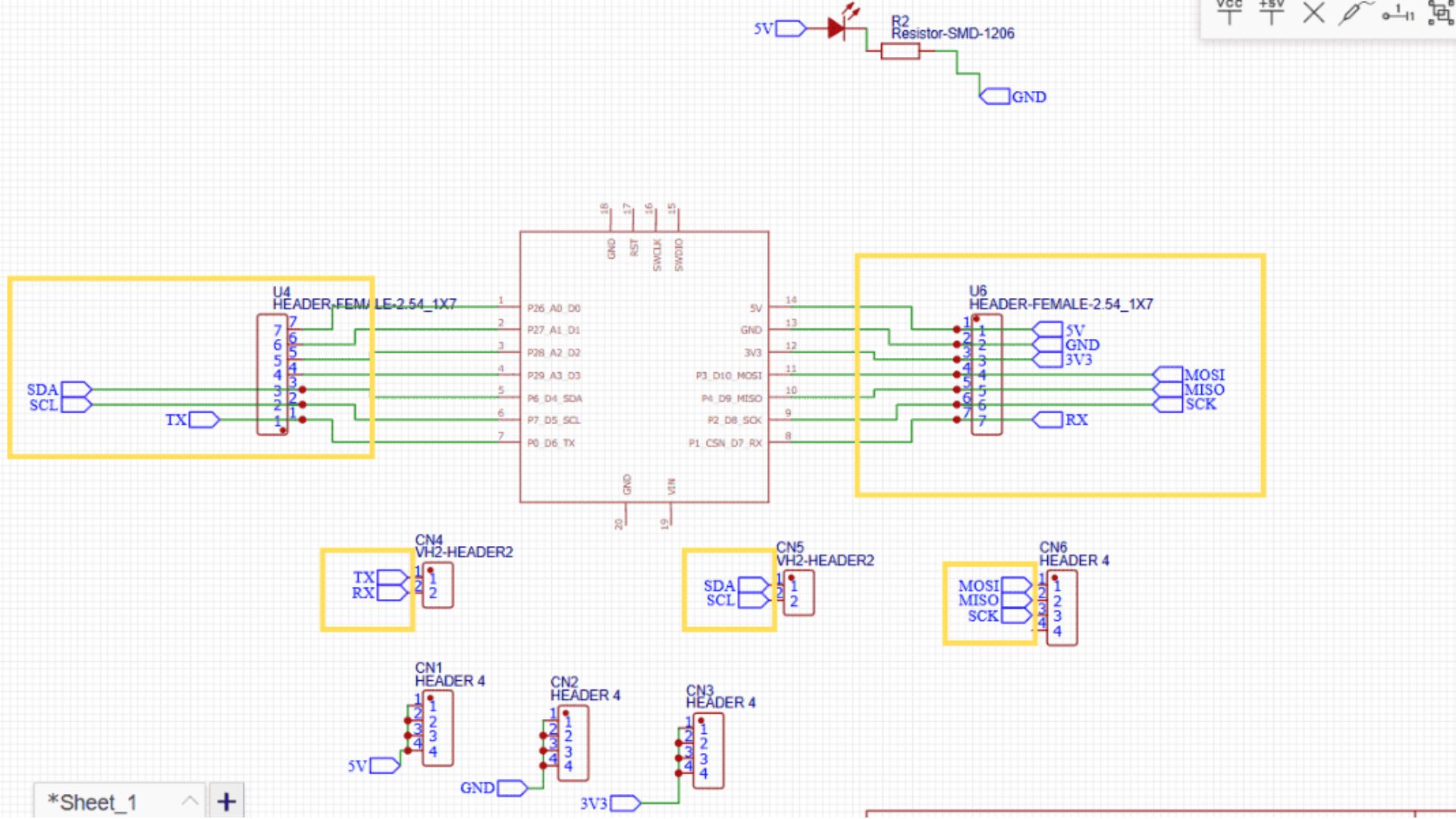
This stage ensured that the circuit logic was correct before moving into physical design.
Component Footprints — Digital to Physical Mapping
Each component in the schematic was assigned a footprint.
This defines:
pad size and spacing
exact physical dimensions of components
soldering contact areas
Care was taken to:
select correct SMD packages
match footprint orientation with real components
avoid mismatches that could cause assembly failure
This step is critical because errors here directly affect fabrication and soldering.
PCB Layout — Tank Form Development
The board was developed in a tank-shaped form, which required careful spatial planning. Components were arranged to fit within the geometry, and traces were manually routed to maintain clear and efficient connections. This stage highlighted the relationship between circuit logic and physical structure, where layout decisions directly affect both performance and form.
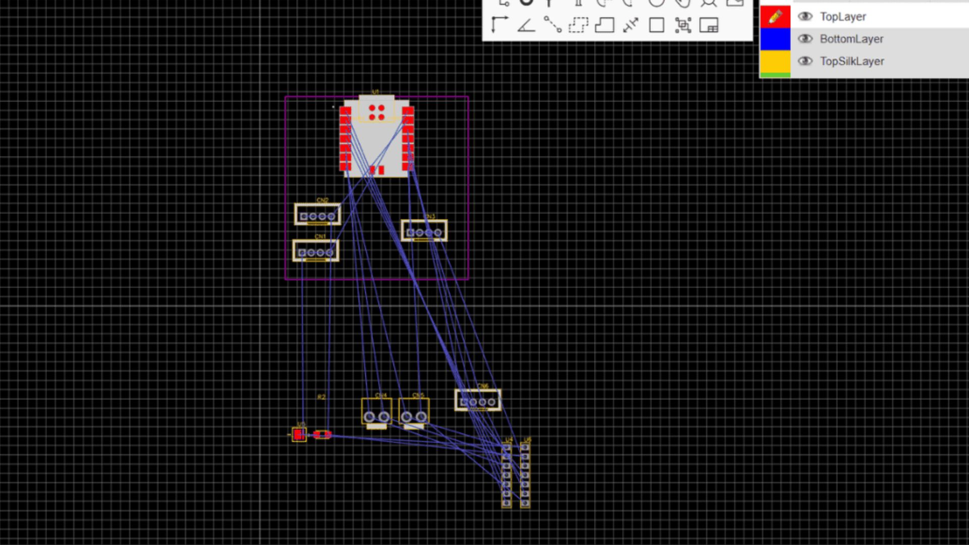
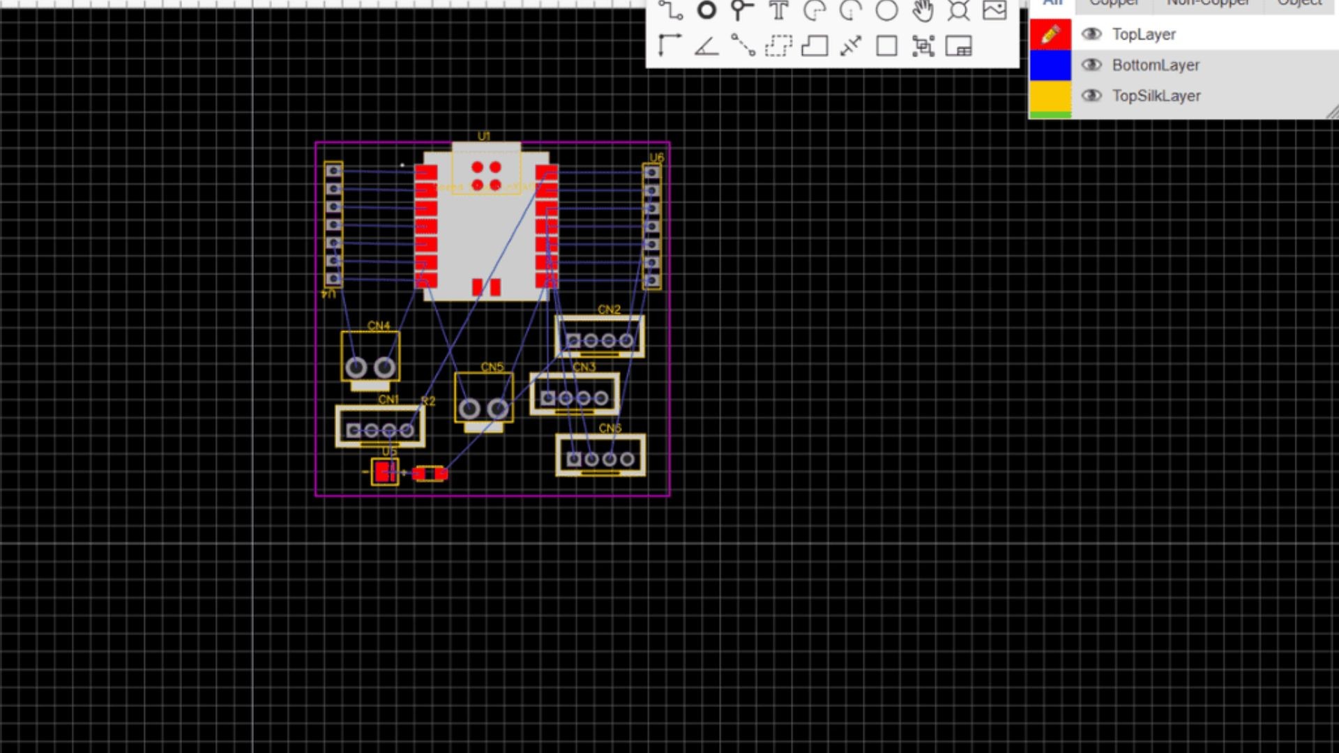
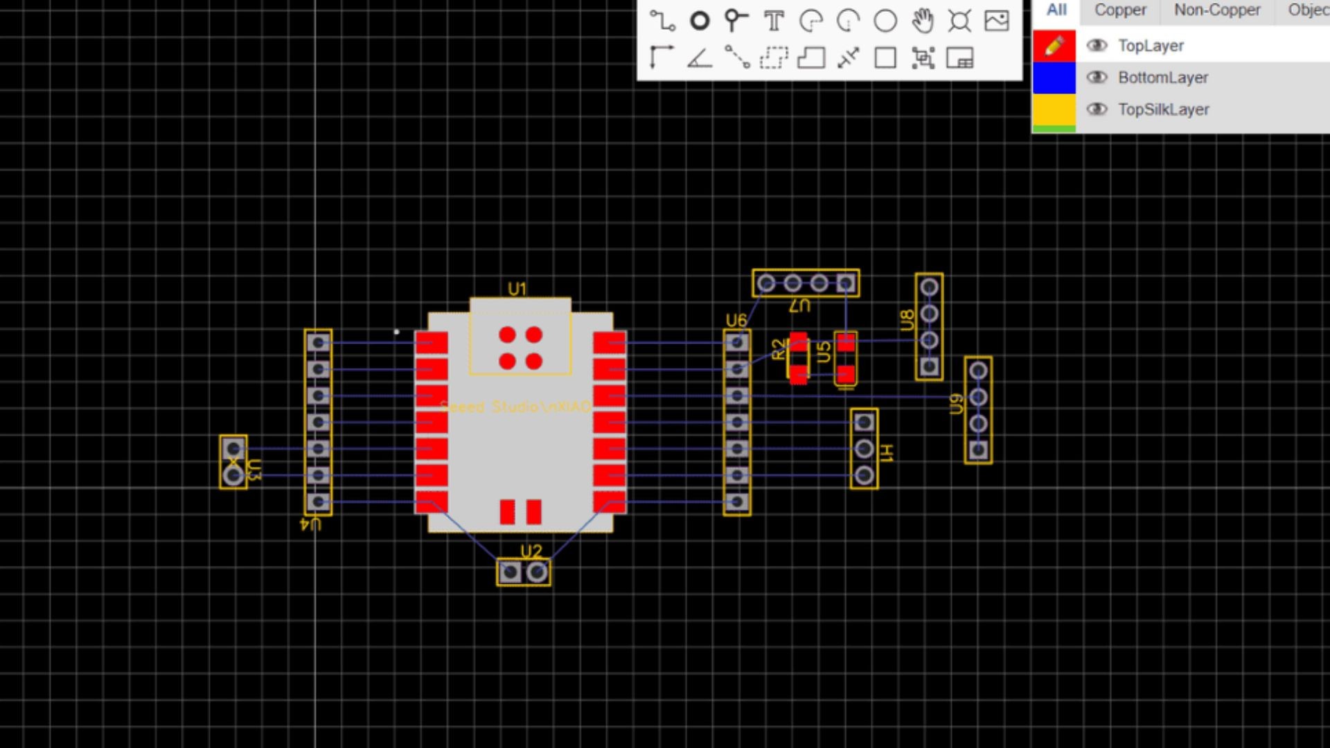
Traces were manually drawn
Short and direct connections were prioritized
Crossovers were avoided due to single-layer board constraints
Trace width and spacing were controlled for milling
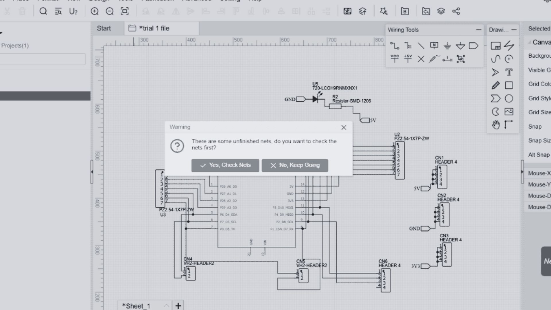
Design Rules & Validation
Before fabrication, the design was validated:
checked connections (DRC)
ensured trace width and spacing were manufacturable
exported files for milling
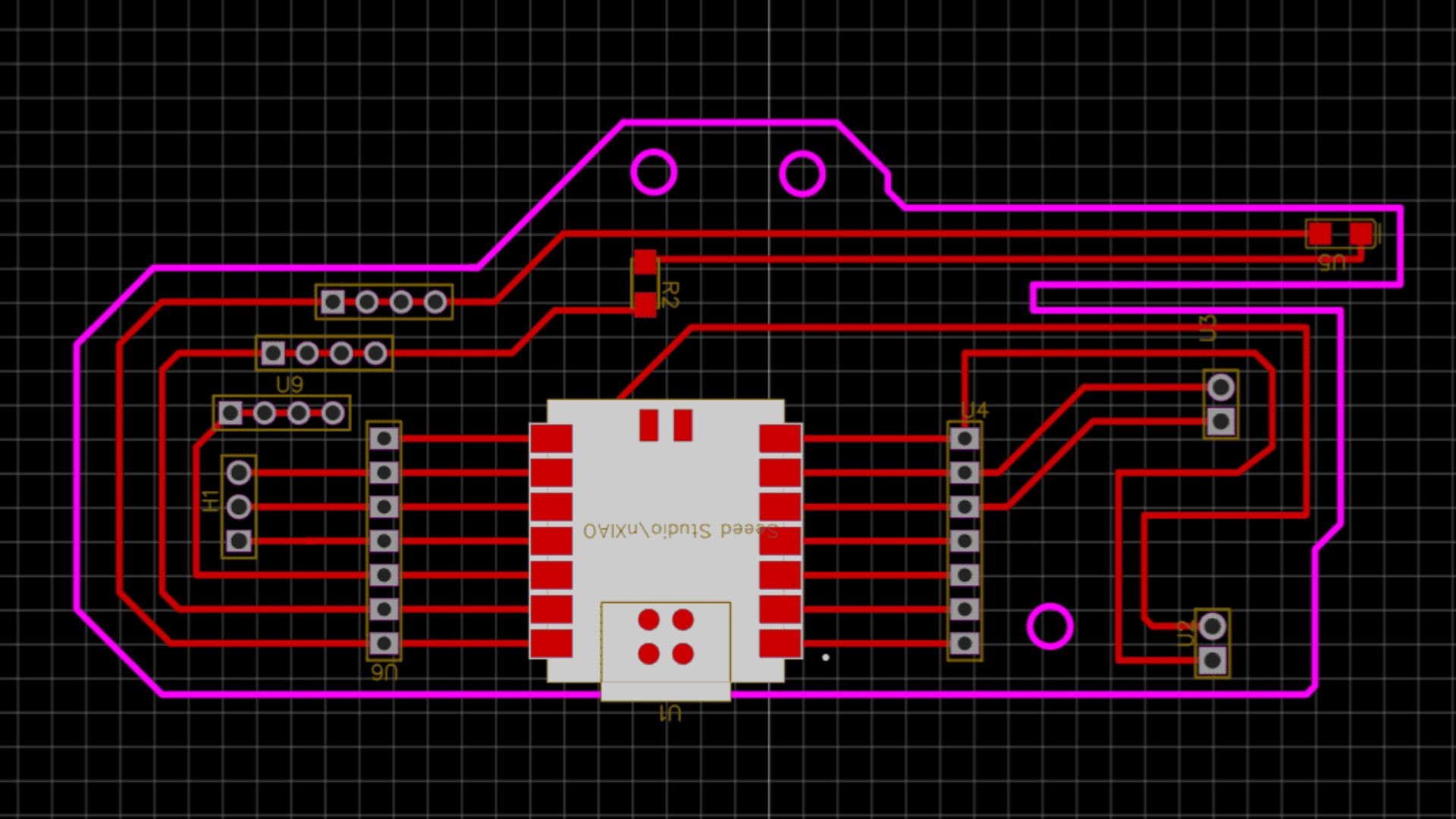
The layout was then exported and converted into toolpaths. Parameters such as tool diameter, cut depth, and offset values were defined to prepare separate operations for trace milling and board cutting. This stage bridged the digital design with machine execution.
File Preparation — Toolpath Generation
Toolpaths were generated considering:
tool diameter
cut depth
minimum trace width and spacing
Separate toolpaths were generated for:
trace milling
board outline cutting
CNC Milling — Fabrication
The board was fabricated using a CNC milling machine on a copper-clad board.
Process:
Board fixed securely to machine bed
Tool zeroed on X, Y, and Z axes
Trace milling performed first (shallow cut)
Outline cut performed after (deeper cut)
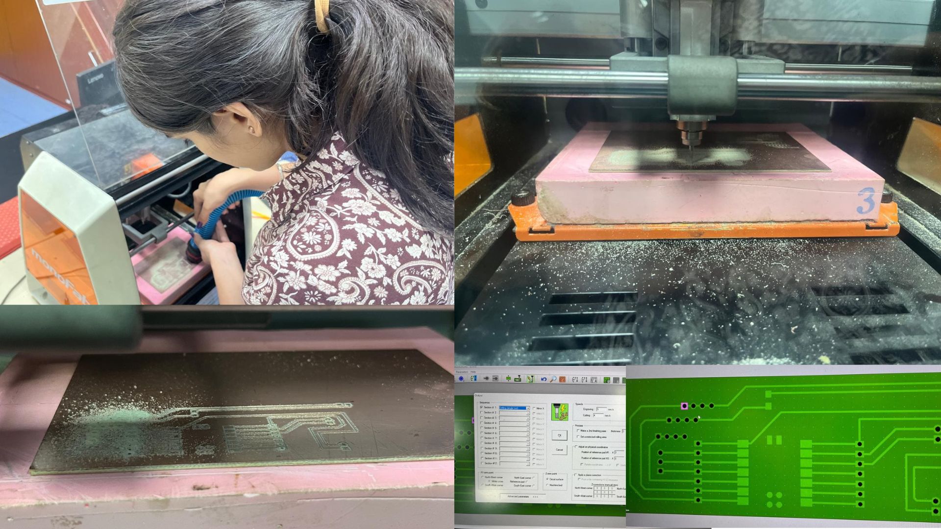
Challenges faced:
incorrect depth could remove traces completely
insufficient depth could leave copper connections
alignment had to be precise
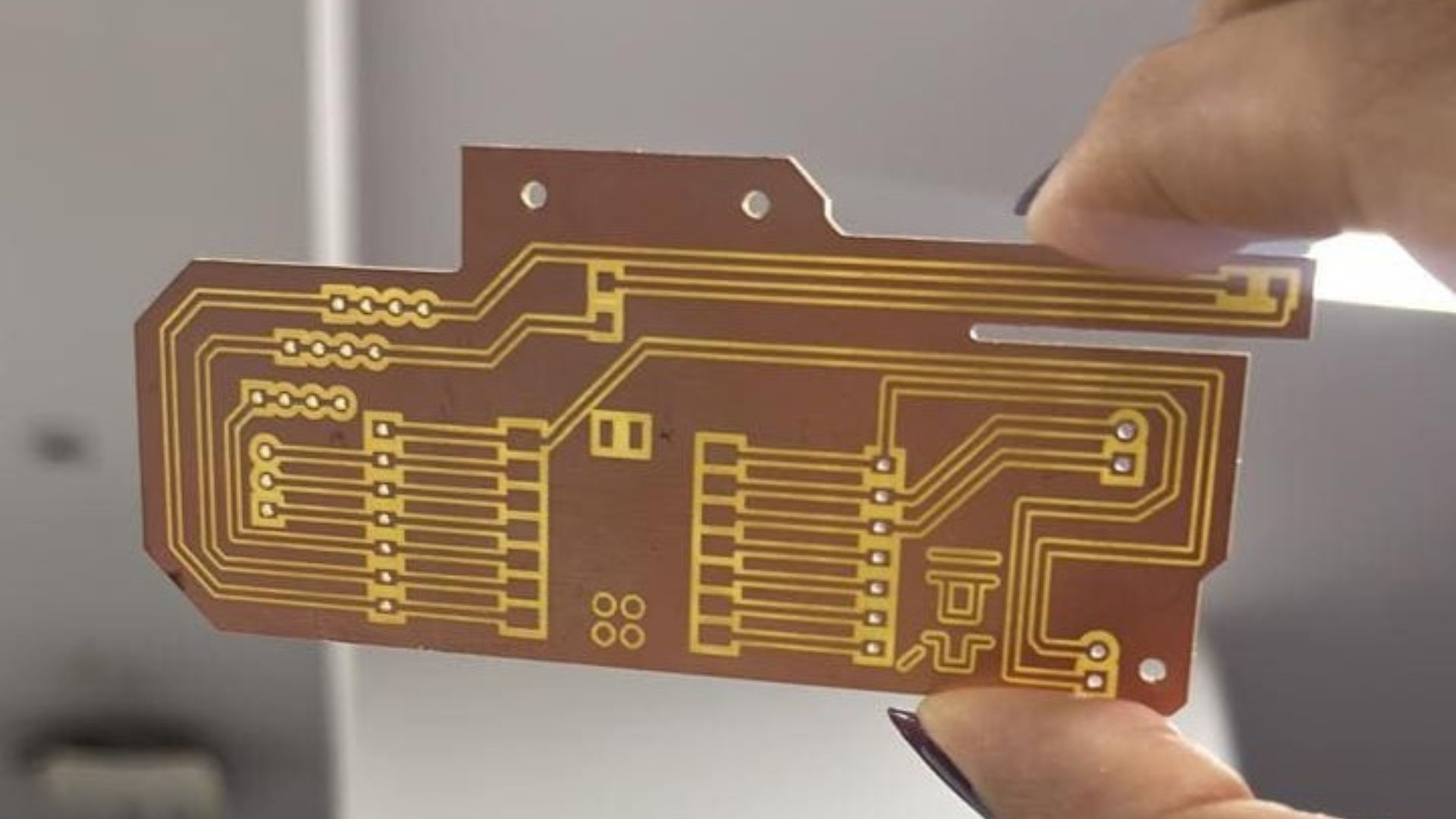
The result was a physically milled PCB with exposed copper traces.
Assembly — Soldering Components
Components were assembled onto the PCB using soldering.
applied solder to pads
placed components using tweezers
heated joints to secure components
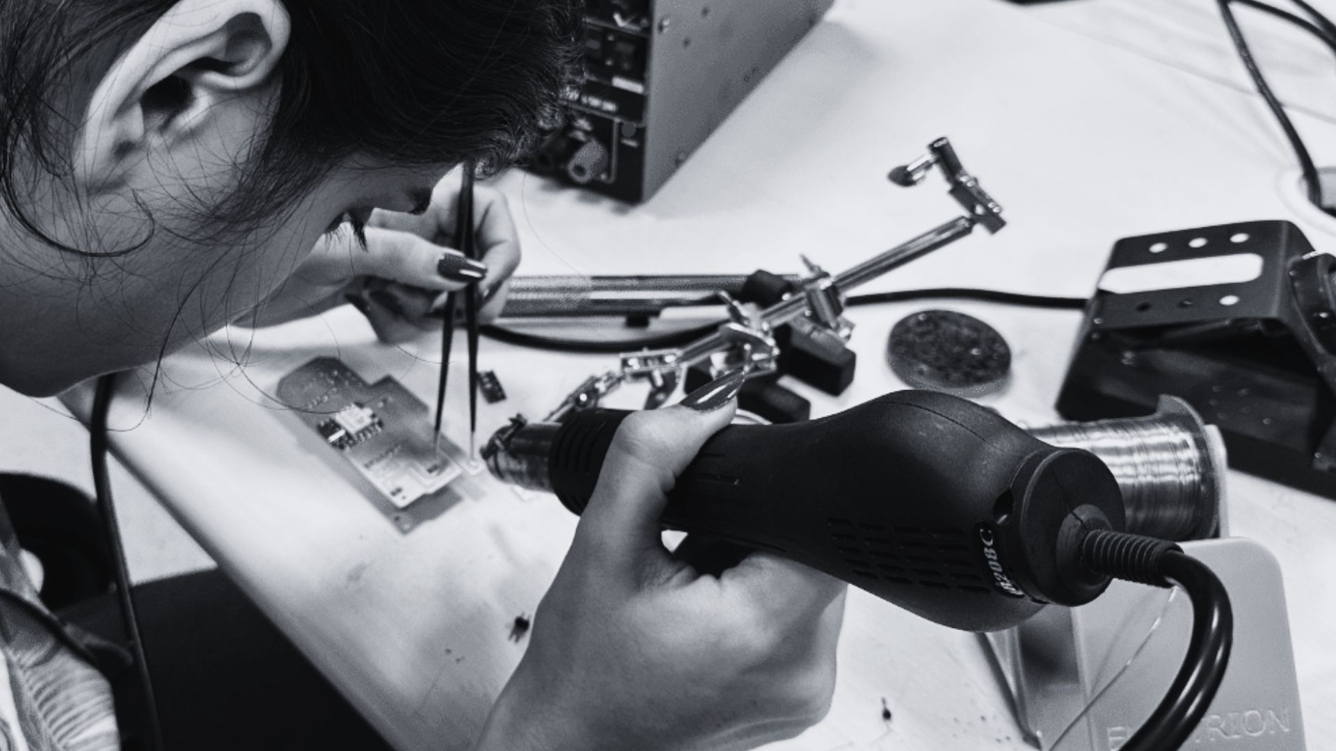
Important considerations:
correct orientation of LEDs and microcontroller
avoiding solder bridges between pads
maintaining clean joints
This stage required precision and steady control.
Testing & Debugging — Functional Validation
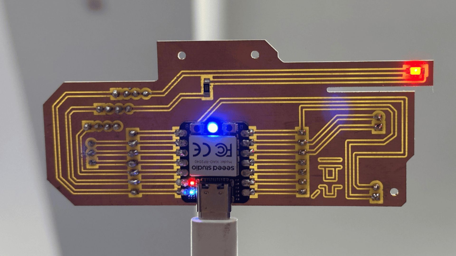
Checked connections and verified that the board functions as intended.
Projects
other

